
Make your own PCBs form A to Z
using Eagle Layout Editor + Photoshop
author: Hlias Hliadis
using Eagle Layout Editor + Photoshop
author: Hlias Hliadis
Making your own PCBs is a procedure that needs extreme care so the result become usefull. Many times you faced up the challenge to print out your own PCBs many times or many different PCBs in one sheet. In this article we will discuss how you can do this compining common software tools. Also we will discuss how to print out PCBs from Elektor magazine along with your own custom made PCB in one transparency, after processing it using Photoshop CS for better results.
The software tools you need are:
- Adobe Photoshop CS (image processing).
- Adobe Acrobat Reader (PDF files reader).
- Eagle Layout Editor 4.11 Freeware (PCB design).
- PCB PDF files from Elektor magazine (available at their website)
see (page 3/3) for resources.
Designing
For the beginning we will design a simple circuit to Eagle which will flash two LED diodes. Open Eagle, under Projects right click and then left click to New Project.

Give a name to the new Project, for example Blinking Led and then click Enter.
Under the Project you created, right click and select New and then Schematic.

Right away the schematic editor will show up Project : Blinking Led

After finishing the circuit design, you must check it out for design faults or not connected components. This can be done clicking Erc
Then we must transfer the design to the PCB design program. This can be done clicking on Board

At this point you must arrange the components as you like, but you should have in mind to put them in places so the shortest route connects them.`
After completing the components arrangement use button Ratsnet

The result is like the PCB shown below.
Autorouter settings 1 TOP [N/A] - 16 Bottom [*]. You leave the rest as is.

When the PCB design is ready it's time to export it to an image file to be able to process it using Photoshop CS.
First of all we must hide the layers we don't need, for example the components, the names, values and let only the PCB traces.
To achieve this we must click on Display Del


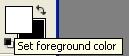 The section you selected in now in a discontinuous line, this section must be filled with black color, to achieve that select select the background color to black


20 Dimension
21 tPlace
22 bPlace
After pressing OK we must see some a screen similar to this one:
Then click File – Export and select Image.
This image will show up:
As more Resolution you choose the best processing will occur in Photoshop CS, also you must check Monochrome box, give a name and click OK.
You must be careful choosing Resolution, because the more dpi has result the best quality but the bigger file size, 300 dpi it's a good resolution for print out.
Example:
File: BlinkLed.bmp
Resolution: 300dpi
Monochrome:
File: BlinkLed.bmp
Resolution: 300dpi
Monochrome:
The result is this:
At this point we no longer need Eagle, the next step it processing the image using Photoshop CS
Processing in Photoshop
Open Photoshop and click Open, find file BlinkLed.bmp and click Open, the program will open the PCB you created using Eagle.
As you can see the PCB traces are white and the empty space is black, that must be inverted because we want to print out the traces.
To achieve this we use the Invert command, click on Image – Adjustments – Invert or use the shortcut keys CTRL+I on your keyboard.
Right away the colors will be inverter and we now have the traces in black and the empty space in white.
As you can see there is an empty white space to the top of the image that is drossy and aggravate the file size , we can eliminate this using Crop Tool
If you wish you can fill the white spaces with black to make a more professional look PCB. To achieve this we must convert the image to Grayscale and create a new Layer. Click on Image – Mode – Grayscale, and the menu Grayscale will show up. To Size Ratio give value 1 and click OK, then click to Layer – New – Layer or use Shift+CTRL+N shortcut from your keyboard.
Creating a new Layer is very important, for the reason that we don't affect the original design and we can restore it to the previous state if we want to.
With the creation of the Layer you will see to the Layers box that you have Background which has a lock and Layer 1.
Click to Layer 1 and select the Paint Bucket Tool
Next click into the design, it will become black, but don't be afraid this is going to change in a while!
Now, double click to Layer Background, and the dialog box New Layer will open and then click OK.
You will see that Background now renamed to Layer 0 and the lock disappears, now click and hold the left mouse button to Layer 1 and drag it under Layer 0, you must be able to see the original design.
At this point we must see some common functions of Photoshop so we can make our lifes easier. Photoshop was selected because is the best program - in my opinion - of it's category, has many facilities on operation, can read PDF files (Elektor gives PCBs in PDF format) and has the best image quality.
You must beaten using Zoom function, Polygon Lasso Tool and Hand Tool. Zoom can be easily controlled with CTRL+ [Zoom in] – CTRL- [Zoom out], Hand tool is used to move into the image to the section we are interested, holding Space and left mouse button, we move the image to the work area (Attention, Hand tool moves the image in the work area, that means that is replaces scroll bars, but Move tool moves the image of the Layer), Polygon Lasso tool is used pushing L, Lasso with the help of Shift button can create horizontal straight lines, vertical and diagonal. You must always finish the Lasso tool to the point it started so it makes a closed loop (like the image below. Experiment with the tools to habituate with their operation. it's better to create a copy of the design so the prototype so you always have a untouched copy, click Image – Duplicate.
Click on Layer 0, Zoom to image 200%, move it with the Hand Tool, select Lasso tool, click near a PCB trace holding Shift key and drag the mouse in the direction of the trace. Follow a go-around to close the loop at the point you started. If you want to move the image use Hand tool.
The section you selected in now in a discontinuous line, this section must be filled with black color, to achieve that select select the background color to black
Repeat the operation to fill all the section you want to be black and finally the PCB will look like this one:
The “filling” could be achievement using Eagle with a Script, but the company that develops Eagle hasn't included a Script like this yet and the user's scripts have many glitches, so we prefer Photoshop to have more flexibility processing our design.
Save the image in PSD format (Photoshop Format ) to be able in future to make any changes.
Now we will open an Elektor's PDF pcb file to process it using Photoshop.
For our example we use a file from the English site of Elektor, in the free category MiniProjects Online, we selected Led Christmas Decoration.
At webpage there is the word more… that links to a PDF file, this PDF must be downloaded (right click "save target as") to you pc.
After you have this file on your hard disk you must open it with Photoshop CS, click Open – File and open the PDF file.
The PDF Page Selector will show up, Inside this you can see the pages of PDF file, we need the one with the PCB layer that's on page 2, click on page 2 and OK.
Now the Rasterize Generic PDF Format dialog box will appear.
At Resolution field you must give the same value as our design has , (if you don't need to attach another PCB file then give a value between 150 and 600 dpi) at this example put 300dpi and click OK.
The file will open in Photoshop's working area.
We must remove any schematic, text and layout we don't need using Crop tool. Select the PCB area and click Enter. Now only the PCB remains.
This PCB must be printed two times for the construction and let's assume we want to make this construction twice. That means we need it four times.
To reproduce the PCB 4 times, we must change the paper size to our original design to Α4, Α4 measures 21*29,7cm (Width: 21 – Height: 29,7), click on Image – Canvas Size… menu
Put values Width: 21 – Height: 29,7 in cm and click OK, now the paper has Α4 dimensions.
At Layer bar there is Layer 1 and this is the Layer we must reproduce, to achieve that click CTRL+A and you will se to the borders of the paper discontinuous lines, then click CTRL+C to copy the Layer to the computer's memory, now click CTRL+V 3 times and you will se at Layer bar 3 Layer more (Layer 2, Layer 3, Layer 4), with Move Tool arrange the layers to the page. The page must look like this one:
The empty space we left at the bottom will be used to add the PCB we created with Eagle Layout.
Open the PCB we made with Eagle to BlinkingLed.PSD file, make a duplicate copy and close the original one. Click on layer menu and select Merge Down ή CTRL+E, you will see Layer 1 and Layer 2 to merge and finally only Layer 1 exists.
Click and drag in Layer bar Layer1 on top Elektor and the Eagle PCB will be added to Elektor's pcbs page along with Layer 5 to the Layer bar, with Move Tool move Layer 5 to the desired destination.
The PCB we created in Eagle is smaller than the Elektor's one but if you retain the Resolution then you must don't scare if you see it smaller. At this point make a test print on Α4 page to see if everything is printed out correctly and try to fit a component on top of the page to see if the scale is the right.
Exposure
If everything is printer out correctly on the test page print it out to a transparency using a Laser printer to the maximum resolution, cut the PCBs from transparency and keep then in a good condition until development. Your hands must be clear and you must don't tough it on top of traces.
You will need:
· Exposure chamber with UV light 300W
· 2 pieces of glass 30x30cm , thickness 0.5mm
· Peridrol (from local pharmacy shop)
· sparse Hydrochloric acid (form Super Market, used in baths)
· Toboflo (from Super Market)
· Plastic gloves
· UV Light sensitive boards
· Protective Laquer spray
· Drill with drill bits form 0,5mm to 3mm
· 2 plastic basins
The exposure chamber isn't difficult to construct, it consists of a box (preferred from wood), with useful height 60cm width and depth 40cm and a door that apply the best way to the box. In a hole to the roof you attach the lamp. The lamp fitting must be from porcelain to prevent melting of it. You can also attach rubber bottom to the box to eliminate vibes that affect lamp's life.
UV lamps emit ultraviolet radiation and are more expensive than regular ones, among this they need a warm up time of approximately 5 minutes to have best performance, so before put the PCB inside let it warm up. ATTENTION: Never look directly to the lamp, it is VERY hazardous for the eyes.
The 2 pieces of glass needed to support the PCB and transparency contact in the exposure chamber, use one piece as base and put the photosensitive PCB on top of it with the copper side up, then put the transparency with the printed side face the copper side of the PCB and then put the second piece of glass on top of all. Use adhesive tape to seal them all together.
All this must be done in a room with no bright lights and make fast movements, because photosensitive boards from the time we remove the protective layer are exposed to any light and you may experience problems if let it to much time exposed.
After lamp warm up, put the two pieces of glass along with PCB and transparency, without looking or touching the lamp, close the door and let it exposed 15 minutes, exploit this time frame to find a cartoon box (p.e form shoes) to put the PCB in after exposure and heat (DON'T BOIL) 1 litter of water.
When 15 minutes passes turn off the lamp and take off the pieces of glasses. Take the exposed PCB and put it inside the cartoon box until the time to etch bath comes.
As you see above I don't use the "classic" enchants (sodium hydroxide – trichoride ) because they are dangerous for environment and human and they are also difficult to deposit them later .You are not allowed to depose them in environment or to the WC but give them to a chemical laboratory. The chemicals I propose can be deposed to drainage (NOT depose them to environment either), apart from that housewives use them for house cleaning.
The etching procedure must take place to a well ventilated place or to open space with the use of plastic gloves and the best attention you can have (have in mind that Hydrochloric acid is an ACID) as you have to manage chemicals!
To one of the two basins put the heated water and 3 spoons of Tuboflo, (you must not use this spool again for food!) mix the solution well until Tuboflo is dissolved.
To the second basin put ¼ of the Hydrochloric acid solution and a little Peridrol (around 2 caps of a common water bottle). Mix them well.
Now put the board to the first basin with the water and Tuboflo and move it until the traces show up (in around 1-3 minutes). When the traces can be seen clearly remove the board and wash it out with pure water into the bath.
After that place the board to the second basin with Hydrochloric acid and Peridrol and move it around until the copper is removed from the exposed areas of the board, (around 15-20 minutes), if the copper removal isn't finished in the time add up 1-2 doses of Peridrol. When etching finished you must have the PCB almost ready with the copped traces only left. You must check the board to see if there are undesirably areas with copper , if you notice that put the board to the solution again until they are completely removed, then wash the board with water and wipe it with toilet paper.
Deposit chemicals to the toilet and wash them also with warm water and soap.
When PCB becomes dry, spay it with the lacquer spray following the manufactures instructions.
When lacquer dries it's time to drill the holes, you will need an electric drill to open the components holes.
If you want a more professional look to your pcb you can do silk screening of components placement, but this is made only to special laboratories and there is an additional cost for it.
At this point the guide has come to it's finish, I hope it helped you a bit to make your own PCBs. Remember, don't be disappointed if the first try fail, patience and persistence are the "tools" to achieve your goals. Good luck.
Hliadis Hlias - vilias@yahoo.com
Electrician - Electronics Engineer
Technician - Industrial Installations
Electrician - Electronics Engineer
Technician - Industrial Installations


PCB Designing Using Eagle Layout Editor and Photoshop
ReplyDeletePCB Designing Using Eagle Layout Editor and Photoshop
ReplyDelete